

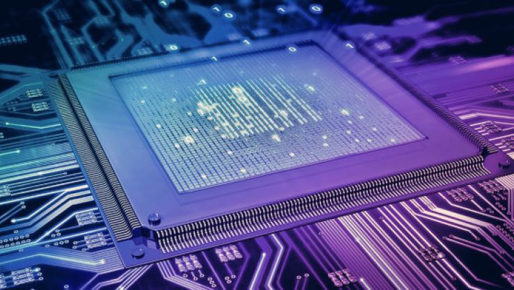
Very-large-scale integration (VLSI) is a procedure of combining large number of transistors into a single chip. It began during the 1970s with the development of complex semiconductor and communication technologies.
Commonly known as a VLSI device, it is the microcontroller. Prior to VLSI, most ICs used to possess the limited functions. An electronic circuit generallycomprises of a CPU, RAM, ROM and other peripherals present on one board.
VLSI enabled the design by allowing IC designers to add all of them into a single chip. Before going into specifics, let’s peek into the VLSI development. Also see how VLSI training institutes in Bangalore and VLSI courses in Bangalore are gradually reshaping the future.
Integrated circuit evolved through the years. Earlier it used to contain few transistors, logic gates, ICs and other few things. However, during the process the number of transistors in an IC dramatically increased.
VLSI technology is one of the most preferred technologies todaybecause of the following advantages:
- The expansion in thickness occurs through different advancements. Some of which would be a decrease in size, the board in power utilization among others,
- Reduces the size of circuits
- Reduces the compelling expense of the gadgets
- Increases the working pace of circuits
- Requires less force than discrete segments
- Higher unwavering quality
- Occupies a moderately littler region
We should investigate the structure nuts and bolts to see a portion of the fundamentals of VLSI working.
Structuring a VLSI IC
The structure of a VLSI IC comprises comprehensively of 2 sections. Front end configuration incorporates computerized configuration utilizing HDLs, for example, Verilog, VHDL, SystemVerilog and such. It incorporates plan check through recreation and other confirmation strategies. The procedure incorporates planning, beginning from entryways to structure for testability. Backend configuration contains CMOS library structure and its portrayal. It additionally covers physical plan and flaw reproduction. The whole structure methodology follows a bit by bit approach. The front end configuration steps would include,
Issue Specification
It is a significant level portrayal of the framework. The significant parameters are execution, usefulness, physical measurements, manufacture innovation and plan strategies. It must be a tradeoff between showcase prerequisites, the accessible innovation and the financial feasibility of the structure. The end particulars incorporate the size, speed, force and usefulness of the VLSI framework.
Engineering Definition
Fundamental determinations like gliding point units, which framework to utilize, RISC or CISC, number of ALU’s reserve size and so forth.
Useful Design
Characterizes the major useful units of the framework and henceforth encourages the ID of interconnect necessities between units, the physical and electrical determinations of every unit.
Rationale Design
Boolean articulations, control stream, word width, register portion and so forth are created and the result are RTL portrayal. HDLs execute the RTL depiction onto a framework.
Circuit Design
While the rationale configuration gives the rearranged usage of the logic,the acknowledgment of the circuit. The netlist comprises of entryways, transistors and different interconnects. This again is a product step and the result is checked through reenactment.
Physical Design
The change of the netlist into its geometrical portrayal is done right now the outcome is known as a format. This progression observes some predefined fixed guidelines like the lambda rules which give the specific subtleties of the size, proportion and dividing between parts.
Back end equipment advancement
Next, we have the equipment execution (or what we study in school). When we sort out the issues with equipment in a reproduced domain, we move onto the genuine equipment. Significantly talking, we have the accompanying strides in equipment creation,
Drawing
It expels material specifically from the outside of wafer to make designs. A drawing veil ensures a few pieces of the material. Extra synthetic substances or plasma evacuates the rest of the photoresist. A review ensures the transference of the picture from cover to the top layer of wafer.
Particle implantation
It is a technique for including dopants. A light emission vitality dopant particles (Phosphine or boron trichloride) is focused at explicit districts of a wafer. The profundity of infiltration into the wafer relies upon the vitality of the bar.
Metallization
A slight layer of aluminum is stored over the entire wafer. Aluminum is functioning as a decent conductor and structures low obstruction contacts. It tends to be applied and designed with single testimony and drawing process.
Get together and Packaging
Every one of the wafers contains many chips. A jewel saw cuts the wafer into single chips isolating the single chips. The chips bombing electrical tests are disposed of, while the great ones are sent for bundling.